Global Non-Volatile Memory Market Analysis with US$ 59.29 Billion Forecast by 2033
The Next-Generation Memory Industry is experiencing steady growth worldwide, driven by the escalating adoption of high-performance computing platforms across diverse technology sectors, a rising global focus on data processing velocity and real-time computing precision, and the pressing need to mitigate power consumption and data transfer bottlenecks in modern enterprise infrastructures.
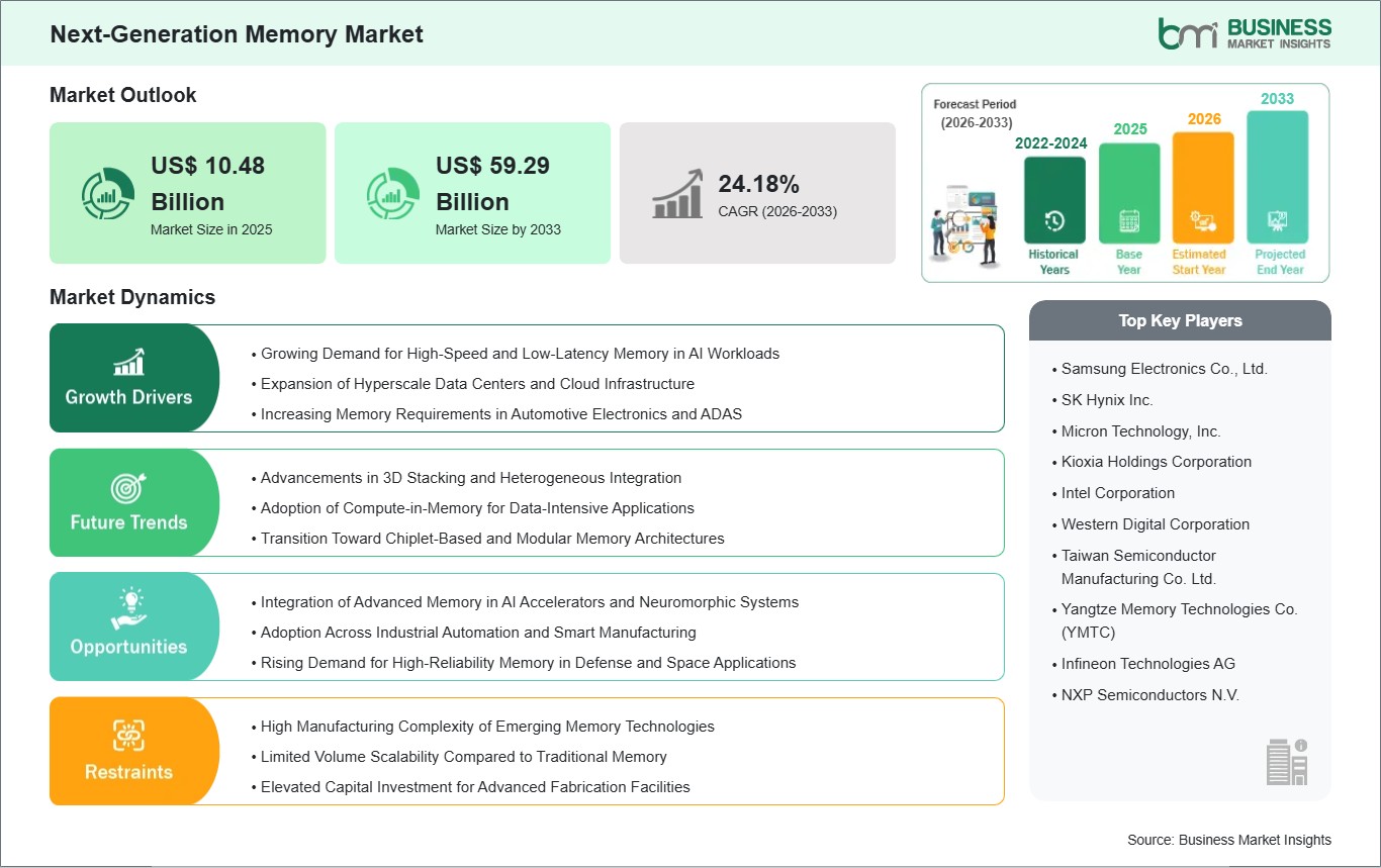
According to Business Market Insights, the global Next-Generation
Memory Market size is expected to reach US$ 59.29 Billion by 2033 from
US$ 10.48 Billion in 2025. The market is estimated to record a CAGR of 24.19%
from 2026 to 2033.
Advancements in three-dimensional (3D) memory architectures,
artificial intelligence (AI) integration in predictive heavy-workload
management, and advanced process node lithography technologies, along with the
rising deployment of high-density storage systems in secondary industries like
automotive telematics and automated industrial manufacturing hubs, are
significantly transforming the market landscape. Semiconductor fabrication
facilities are increasingly prioritizing extreme thermal resistance, flexible
ultra-low latency interfaces, and cloud-connected chiplet diagnostics to meet
shifting regulatory preferences for energy-efficient data storage frameworks
and zero-error processing turnaround.
What Is Next-Generation Memory?
Next-generation memory encompasses a comprehensive range of
advanced, high-speed, multipurpose electronic storage architectures
programmable across computing hardware networks, designed for heavy-duty system
automation and data tracking applications. Their primary objective is to
execute highly continuous, precise, and power-efficient recording of complex
data arrays and machine instructions at high speeds without manual hardware
reconfiguration bottlenecks.
Because modern digital management demands continuous
operational transparency and zero-defect data transmission control,
next-generation memory frameworks are extensively deployed across consumer
devices, cloud enterprise servers, and automated vehicle electronics.
Traditional computing configurations relied strictly on rigid, legacy volatile
storage components enclosed in localized motherboard slots. In contrast,
advanced next-generation memory configurations integrate sophisticated
non-volatile solid-state materials, deep-learning memory controller algorithms,
and advanced interface standards tailored to handle delicate peak-data
processing surges and dynamic, variable processing grids.
Download Sample Report: https://www.businessmarketinsights.com/sample/BMIPUB00032364
Market Drivers
A primary driver for the Next-Generation Memory Industry is
the rapid automation and digital transformation of the global cloud computing
and high-performance data processing sectors, particularly in the production of
hyper-scale server clusters and complex artificial intelligence training
networks. These high-tech computing fields require sub-nanosecond precision in
read/write operations and real-time cache optimization that traditional silicon
tracking methods cannot consistently achieve.
The rising operational overhead and widening skilled
engineer shortages across major microelectronics fabrication divisions also act
as a vital growth factor. Implementing automated 3D memory architectures allows
manufacturing fabs to run continuous, optimized production cycles, helping
companies maintain high chip yields while shielding their operational overhead
from global materials supply chain market volatility.
Furthermore, stringent environmental protection regulations
and corporate sustainability initiatives aimed at reducing data center
electricity consumption significantly contribute to market demand. The growing
transition toward deploying specialized low-power chips for eco-conscious
setups such as green data center infrastructures, smart grid monitoring
nodes, and electric vehicle ADAS computing boards is heavily driving market
volume.
Additionally, the increasing financial accessibility of
advanced process node wafers and standardized plug-and-play memory controller
components is prompting small and medium-sized semiconductor design houses to
adopt innovation, removing the historical barrier of high upfront capital
design investments and further propelling sustained market growth.
Market Segmentation
By Technology
- Non-Volatile
Memory
- Volatile
Memory
By Memory Interface
- DDR/LPDDR
- PCIe/NVMe
- SATA
- Others
(CXL, UCIe)
By End-Use Device
- Consumer
Electronics
- Enterprise
Storage and Data Centers
- Automotive
Electronics and ADAS
- Industrial
IoT and Manufacturing Automation
- Aerospace
and Defense
- Healthcare
and Medical Devices
The non-volatile memory segment dominates the market due to
its high flexibility, extensive historical enterprise integration, and
established track record of handling diverse data persistence requirements in
cloud servers and consumer electronics sectors. The enterprise storage and data
centers segment is witnessing the fastest growth, heavily supported by its ease
of high-capacity array programming, lower energy dissipation profiles, and
ability to operate safely alongside complex artificial intelligence infrastructure
networks without computational performance barriers.
Regional Insights
- Asia-Pacific dominates
the Next-Generation Memory Industry, driven by rapid industrial
development, massive semiconductor production projects in Taiwan, South
Korea, and China, and heavy government subsidization of local
microelectronics manufacturing initiatives.
- Europe exhibits
steady growth, heavily regulated by strict digital infrastructure
efficiency mandates and a strong regional focus on macro-level energy
conservation goals that encourage the deployment of certified low-power
and integrated memory chipsets.
- North
America accounts for a substantial market share, supported by
high capital investments in artificial intelligence data center
replacement, the accelerating implementation of high-performance edge
computing ecosystems, and strong demand for advanced computing cyber-security
solutions.
- Middle
East & Africa and South & Central America are
gradually expanding due to escalating investments in modernizing urban
digital communication hubs, reducing transmission latencies and data
center power losses, and concentrated efforts to upgrade regional
enterprise IT infrastructure.
Top Players in the Next-Generation Memory Industry
The market is highly competitive, with leading manufacturers
focusing on R&D investments, strategic embedded memory IP developer
acquisitions, and expanding their global foundry maintenance networks to
optimize long-term wafer manufacturing lifecycle stability.
- Samsung
Electronics Co., Ltd.
- Micron
Technology, Inc.
- SK
Hynix Inc.
- Kioxia
Holdings Corporation
- Infineon
Technologies AG
- Intel
Corporation
- Western
Digital Corporation
- Fujitsu
Ltd.
- Everspin
Technologies Inc.
- Avalanche
Technology Inc.
These companies continue to invest heavily in advanced
electronic engineering and hardware-software integration systems to produce
tailored computing solutions that meet the exact data retention, physical
reliability, and software interface interoperability requirements of their
global enterprise and consumer electronics clientele.
Technological Innovations
Technological advancements in chiplet architectures and
materials science are significantly transforming the Next-Generation Memory
Market. Manufacturers are optimizing modern storage arrays by integrating novel
resistive and magnetoresistive materials capable of high-density integration,
enabling systems to dynamically execute edge computing logic and correct
bit-flip errors in real time.
Furthermore, innovations in Compute Express Link (CXL) and
universal chiplet interconnect tracking are gaining traction. Memory design
houses are increasingly commercializing high-efficiency interface layouts that
allow memory blocks to orient, identify, and transmit critical telemetry
signals across heterogeneous processing units, completely removing the need for
structured localized motherboard bus positioning.
The development of integrated digital twin fabrication lines
is also opening new frontiers, allowing semiconductor engineers to completely
simulate, test, and debug entire silicon wafer manufacturing flows virtually
before deploying physical lithography masks to the fab floor, minimizing costly
production disruption downtime.
Future Market Outlook
The future outlook for the Next-Generation Memory Industry
remains highly positive. As global supply chains increasingly prioritize
high-performance computing resilience, operational agility, and sustainable
energy management, the electronics sector will continue to transition away from
legacy volatile architectures toward highly adaptive, modular next-generation
memory layers.
The ongoing expansion of subscription-based
"Storage-as-a-Service" (SaaS) business models, alongside the rising
integration of Compute Express Link protocols for ultra-low latency server
cluster coordination, is expected to create substantial growth opportunities.
Manufacturers that prioritize seamless chiplet plug-and-play analytics, robust
hardware-level security firmware encryption, and lightweight, low-power
processing-in-memory architectures will be best positioned to capture market
share in the coming years.
Frequently Asked Questions (FAQs)
What is the difference between next-generation
non-volatile memory and traditional NAND flash memory?
Traditional NAND flash memory relies on trapped electrical
charges that degrade over time and suffer from high write latencies. Advanced
next-generation non-volatile memory options, such as MRAM or ReRAM, utilize
physical state alterations (like magnetic orientation or resistive filaments)
to deliver significantly faster write speeds, near-infinite operational
endurance, and a drastically reduced energy usage profile.
What is a high-bandwidth memory (HBM) chip best used for?
High-bandwidth memory chips feature vertically stacked DRAM
dies connected via through-silicon vias (TSVs), making them highly efficient
for rapid artificial intelligence model training, high-performance
supercomputing, and complex graphics rendering operations across high-density
enterprise data center networks.
How does a digital twin help in next-generation memory
manufacturing?
A digital twin is a virtual replica of a physical
semiconductor fabrication line and its lithography parameters. It allows
microelectronics engineers to program, optimize, and stress-test chip yield
curves and process node variation limits in a digital space, ensuring zero
structural defects and saving significant time during actual physical silicon
production rollout phases.
Can next-generation memory modules operate in extreme
weather conditions?
Yes, many manufacturers produce specialized ruggedized
next-generation memory modules. These systems feature fully sealed,
high-temperature tolerant materials and robust solid-state architectures
designed to prevent thermal breakdown and heavy radiation-induced bit flips,
making them suitable for harsh aerospace deployments or sub-zero automotive
applications.
Browse More Reports:
About Us
Business Market Insights is a market research platform that
provides subscription service for industry and company reports. Our research
team has extensive professional expertise in domains such as Electronics &
Semiconductor; Aerospace & Defense; Automotive & Transportation; Energy
& Power; Healthcare; Manufacturing & Construction; Food &
Beverages; Chemicals & Materials; and Technology, Media, &
Telecommunications.
Contact Us
If you have any questions about this report or would like
further information, please contact us:
Contact person: Ankit Mathur
Email: sales@businessmarketinsights.com
Phone: +16467917070


Comments
Post a Comment